|
Virtuoso Tutorial:
Getting Started
Version
1.2 |
www.berkeley.edu
© 2006 University of
California - Berkeley
Virtuoso Tutorial Version 1.2
Welcome to Virtuoso, the full custom
layout editor from Cadence, Inc. Virtuoso is more than just a simple layout
editor. It is a complete layout environment. Virtuoso Features
- Interactive viewing and
editing of hierarchical layout
- Hierarchical and incremental
DRC
- Built in netlisting
- Interactive connectivity
tracing
- Interactive wiring tool
- Interfaces to other tools,
including schematic capture (e.g. Analog Artist), and batch DRC and LVS
(e.g. Calibre)
- Smart palette for easy
control and feedback on layers
- Full customization and
extension via Tcl/Tk scripting language and API
- Technology independence via
technology description files
- Optimized for large databases
- Very Fast Redisplay for Whole
Chip Viewing and Inspection
- Reads/writes GDSII
- Runs on Solaris and Linux
operation systems.
This tutorial is based on the North
Carolina State University Cadence Design Kit (NCSU CDK). The tutorial will
introduce you to some of the features. Consult the Virtuoso Manual and on-line
documentation for further information. Starting up Virtuoso
From the icfb window, bring up Library
Manager from the Tools menu (select Tools/Library Manager; automatically starts after
starting icfb)
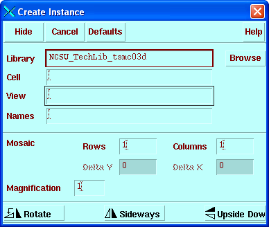
In the Library Manager, create new
library called ee141_lab2 (select File/New/Library). This will open new dialog window,
in which you need to enter the name of your library, library path, and "Attach
to existing tech library" (TSMC 0.24u should be selected). After you fill this
all out, the window should look something like this:

Click "OK"
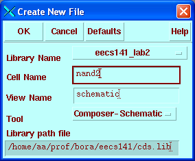
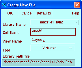
- Create layout view of your NAND
cell. Simply type in "nand2" under cell name and "layout" under view. Hit
"Enter", following window will pop up:
Select "Virtuoso" tool, View Name is automatically set to "layout"
After you hit "OK", Virtuoso screen will appear as shown below (in
addition, LSW window with various mask layers will automatically pop
up):
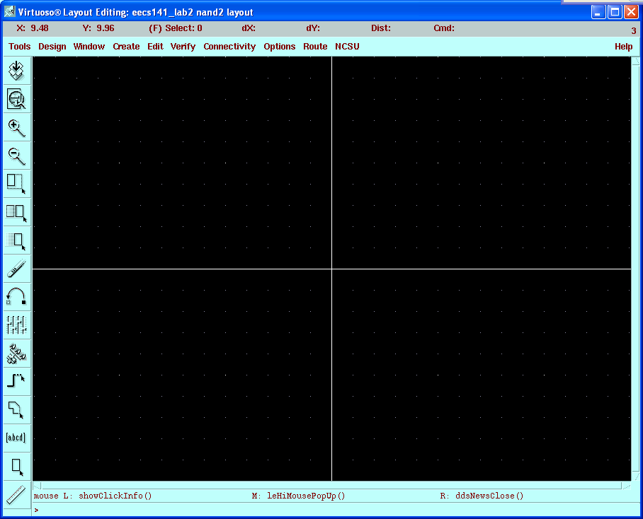
In this window, you will place transistors, draw mask layers
etc.
Virtuoso Screen Layout
On the very top of the window the title
bar should say " Virtuoso Layout Editing: ee141_lab2 nand2 layout
".
This means that you are editing
layout view of nand2 cell from ee141_lab2 library. Next, across the top you should see
the menu bar which contains the following menu items: Tools ,
Design, Window, Create, Edit, Verify,
Connectivity, Options, Route and Skill . These are
pull-down menus much like any PC or Mac application.
At the bottom of the window is the
Virtuoso Message Area . It is activated when some work is in progress
describing the task being performed. It can say something like " Select
the figure to be stretched... ". The Virtuoso Message Area is a sort of
mini-help feature.
The Palette
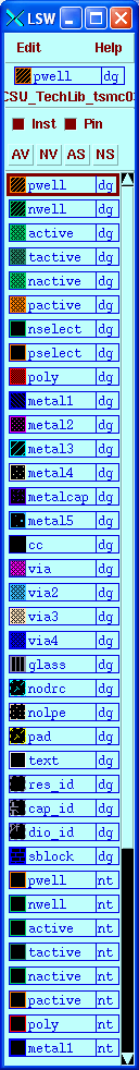
LSW window is the Smart Palette. The
Smart Palette provides many features.
- It controls which layers are
visible, and lets you choose layers for "painting".
- It gives feedback on what is
currently under the cursor, and what is currently selected.
- It allows you to control which
layers can be selected.
Layers
Description of various mask layers can
be found at: <file:/usr/eesww/cadence/NCSU_CDK/doc/layerInfo.html>
Note: you can access this file only from your Unix account.
Use drawing (dg) layers for drawing transistors.
Getting Help
Before we go any further, here is how to
get help if you ever need it.
There are several levels of help
available "on-line" to Virtuoso users. You already know about the quick Help
listed in the Vistuoso Message Area . In addition, you can access the
complete on-line manual, the complete list of active hot-keys, and complete
documentation on text commands at any time.
Before proceeding you should bring up
the Virtuoso Manual and see what's there. The manual is the reference to
Virtuoso and it contains lots of information that you will not find in this
simple tutorial.
Simple Layout
OK, let's get started on some
layout.
- Go to the Virtuoso window and hit
"i" (instantiate)... . This will bring up the following window, click
on "Browse" and select "NCSU_Tech_Lib_03d":
Next, select "nmos" from the NCSU_TechLib, the selection should look like
this:
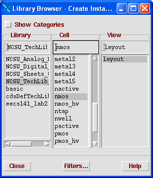
Click Close and then go back to the previous
window and click Hide, position your cursor in Virtuoso
window where you want your nmos placed and click.
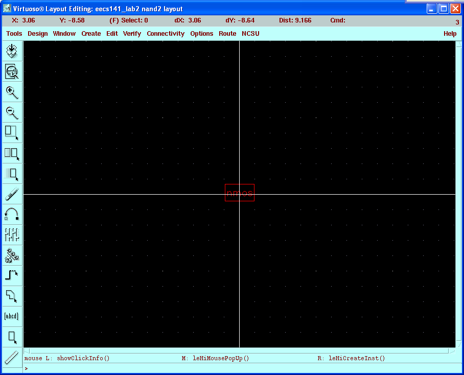
Now, you will notice that Virtusoso works with grid, which is by default very
crude. Also, you don't immediately see what is inside nmos symbol. Let's
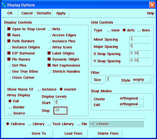
fix this: from the Virtuoso Options menu, choose Display and set
Display Levels from 0
to 10, and also X and Y Snap Spacing to 0.06 (this 0.06 is
half-lambda, lambda is 0.12 in this 0.24um technology). Your display settings
should be as follows:
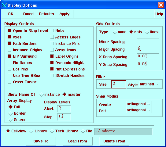
Click Save
To and then OK. Now you can see mask layers in the nmos,
you will later realize that you will be able to place your components on a grid
with much finer precision, the precision of half-lambda (0.06).
Your nmos transistor probably looks very small on the screen, hit
z (zoom in), then
hold left mouse button to select the area you want to zoom in. The
zoomed-in nmos should look like this:
Note that only "active" layer is used and this is OK. (There is no
p-well since this is p-substrate process.) Read more about layout macros (also
known as pcells) such as nmos at
file://usr/eesww/cadence/NCSU_CDK/doc/cdsuser/virtuoso.html#tagpcell
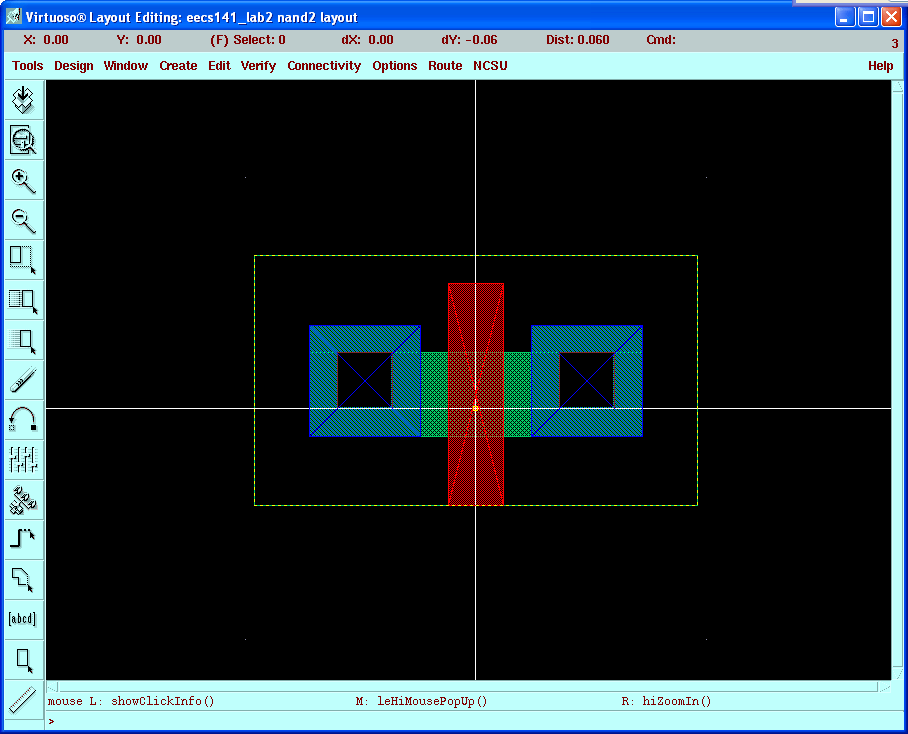
Now, edit instance properties, click on the nmos, when the transistor is
highlited, hit q. Click on Parameters and change the width to 1.98u (2.0u
will be automatically changed to 1.98u due to the grid rules). Since we
eventually want to use this device to make a 2 input NAND gate, change fingers
to 2.
Now Click OK.
Two nfet's merged (stacked) together
should appear.
- Type f ( the hot key for
fit all -- zoom to fit under the Window menu) and the
layout should appear centered in the window.
Your screen should now look like:
TIP! You can undo whatever you have just
done in Virtuoso. Use the u hot key or select Undo from the
Edit menu. You can also Redo what you have just undone using
the Shift-u hotkey.
Zooming
- Now zoom back by typing shift-z, or
use Zoom out in the Window menu.
There are several methods for zooming
found in the View menu.
One easy way to zoom to the exact
region you want is by using the zoom hot key.
- Type z. This puts you in
zoom mode. Note that the cursor has changed. Next hold down the left mouse
button (Button-1) and "drag" out a box which surrounds the region you wish
to zoom to. When you release the mouse the screen will zoom to where your
box was.
- If you mess up don't panic.
Remember, f will always zoom to fit.
The hotkey shift-z can be used to
zoom out by a factor of two.
Selecting and Moving Layout
When Virtuoso is in main mode (the
default), if you simply drag out a region while holding down the left mouse
button (Button-1), whatever is within the box will be selected when you
release the button and will be highlighted in white.
- Drag a box over the stacked nfet's
we just drew. When you release the mouse button, whatever is "selected", in
this case the fet cell, will be highlighted.
Once you have selected an object or
paint you can do lots of things with it.
- For example you can move
it by typing the m hot-key. You can move layout up/down/left/right
one grid at a time by clicking at the selection and moving the mouse. Try
it.
You can also select objects or paint by
clicking on them.
- Clicking the left mouse button
once on a piece of paint selects that particular rectangle of paint.
- Clicking once on a polygon or
cell will select the object.
Duplicating Layout, Cut, Copy and
Paste
Virtuoso supports Cut, Copy, and Paste in the
same format you would see on any good Mac- or PC-based drawing or painting
program.
TIP! All of the zoom,
move, cut and paste, rotate, etc. features that we just executed using hot
keys also have menu equivalents which can be found in the Edit
menu.
DRC
To perform a Design Rule Check (DRC),
choose Verify/DRC.
The DRC form appears:
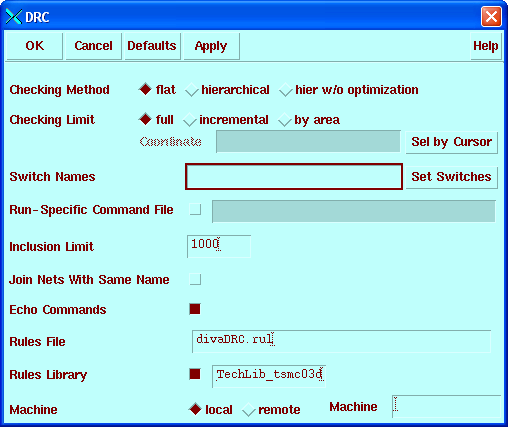
Click OK to run DRC. There shouldn't be any errors marked on the
screen.
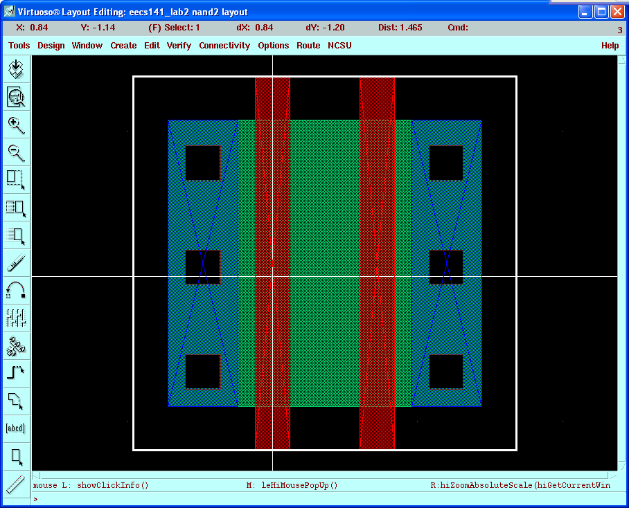
Now, add a pmos transistor with a width of 4 microns and Multiplier equal
to 2. Place it close to the nmos as shown below:
Choose Verify - DRC and hit OK. You will likely see some DRC errors, marked
as white lines on the screen.
Viewing DRC Errors
Use the Verify - Marker - Explain to see more details about flagged
errors.
Errors are described in the marker text window like this one.
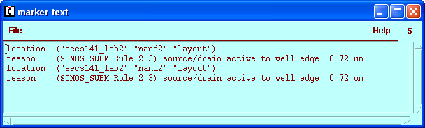
In this particular case, Source/Drain active was too close to the n-well
edge. Minimum required spacing of 0.7um is required. Fix this error by moving
up the pmos.
Esc cancels the explain command, the marker text window will disappear. To
remove error flags, choose Verify - Marker - Delete all
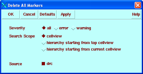
Hit OK to delete all error flags.
Painting
We are now going to "paint" a piece of
poly to connect the pfet and left nfet gates together.
- Select poly layer from the palette,
hit r to draw a rectangle and draw the poly area. Your layout should
look like this:
Wiring
Using r and p hotkeys to
draw rectangles and paths, wire up the two left contact regions and add the
connection to the right pfet contacts. If you have trouble with the p
command see the next section for some hints. Consult CDK manuals if needed.
Your layout should look like this (practical advice: run DRC check
periodically to make sure you're making progress in good direction):
- Type F2, or select Save from the Design
menu (also a good thing to do occasionally).
Adding the Power Rails
Let's say we were laying out this NAND
gate for a standard cell library. Furthermore, assume that the power and
ground rails are run in metal 1 (M1) and that they are 2.04um wide (2.0um
won't work because of the grid granularity, which is
0.06um...).
- To add the M1 power and ground
wires:
1) Set metal1 as an active layer in the LSW window.
2) Type p to bring up the "Create Path" menu.
3) Set "Width" to 2.04.
4) Draw the path where you wish to place Vdd.
- You can always select again the
path you drew and type q to change its properties.
TIP! You can change the size of a path or a
rectangle by stretching an edge using the Stretch command found in the
Edit menu. Simply type s. The cursor changes to let you know
you are in Edit Edge mode. Now move the finger over the edge you wish to
stretch. A line will show you which edge you are over. Once you have the
edge you want click the left mouse button (Button-1) and move the mouse in
the direction you wish to stretch the edge. (Note that in a path you can
change only the length this way - for the width use q and the
properties menu).
Once you have drawn the top power line
you can simply copy it and move it down.
Now that you have laid out your
power and ground rails you should wire them up using the wiring mode as
before.
When designing various cells (nand, nor, inv)
keep the overall cell height constant.
Your cell should look like this:
Wiring Mode - Changing Layers
Notice that the inputs and outputs are
all found within the power straps. What if they need to be brought out so a
router can get to them?
Let's assume the router requires all
signals to be at the top of the cell and in M1. You need to route the poly
wires over the M1 power straps and then change to M1.
Virtuoso can make this job easier
since it can insert all the contacts necessary to go from one layer to
another. For example, if you need to go from poly up to M1, then you simply
start drawing a path (type p) in poly, then click the left mouse button
somewhere close to where you want the contact to be and change the layer in
the "Create Path" menu to "metal1". What you see is that the tip of the wire
turns into a contact, which you can place. Now you can continue to draw your
path in the new layer.
Using the p command, extend both poly lines over the Vdd strap and
end them with M1. Your layout should now look like this (run DRC to make sure
it is DRC-clean!):
Labels
There is one last thing before we are
finished with our NAND gate.
It would be very useful to add pins
with text labels on our layout. To add a pin with a text label
simply select, Pin... from the Create menu.
Click the button next to "shape pin" to open the
Create Shape Pin form:
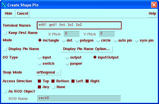
In the Create Shape Pin form, type the following in the Terminal
Names field:
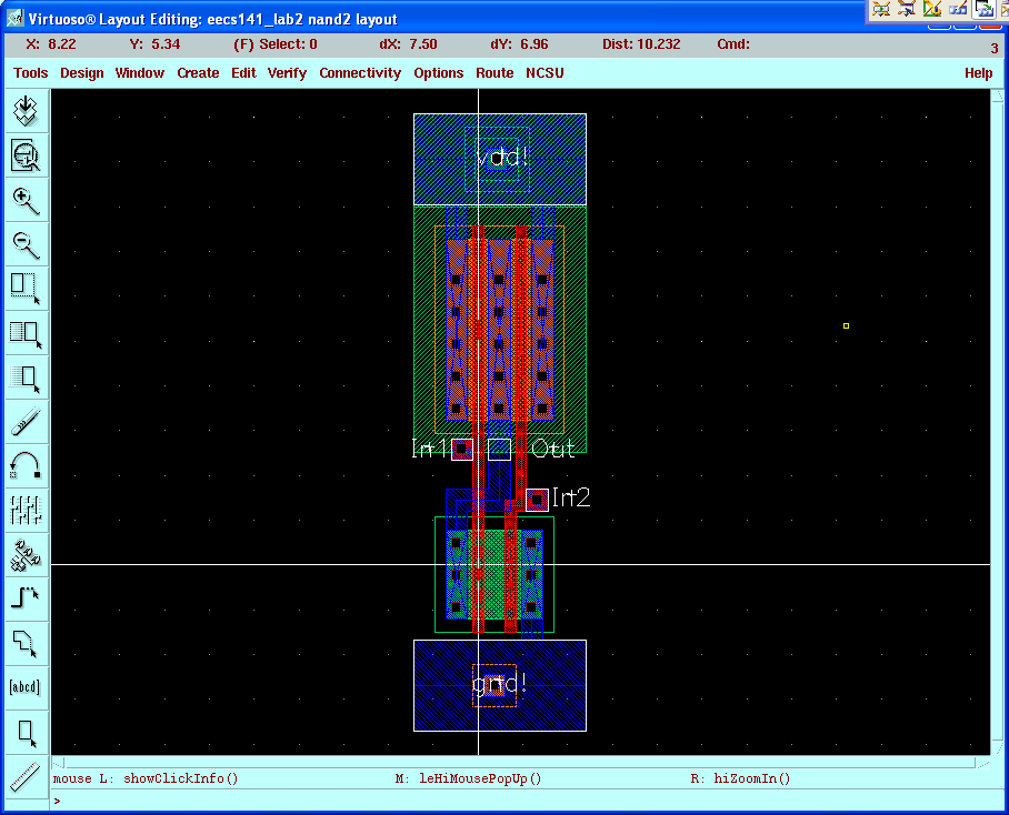
vdd! gnd! Out In1 In2
Click Display Pin Name to associate the name with the pin.
1) Create the rectangle for the vdd! pin coincident with the power line at
the top of the NAND. (start the vdd! pin at the lower- left corner and finish
the vdd! pin at the upper-right corner).
2) The name vdd! appears near the cursor after you click the second
corner (the upper-right corner).
3) Move the cursor to place the vdd! text at the desired place, then click
to place the pin name there.
4) If the text looks too big you can select it, type q to bring up
the property box and edit its height.
Continue with steps 1-3 above to create other pins in specified sequence
(vdd! gnd! Out In1 In2). After you are done, your layout should look like
this:

Our little NAND gate example
should now be done.
Finishing Cell
We are getting ready to finish this
cell. You should add substrate and well contacts (Hint: use ptap and ntap
p-cells). You can try to make the cell as compact as possible, so it can
be tightly abutted.
Your layout should now look
similar to this:
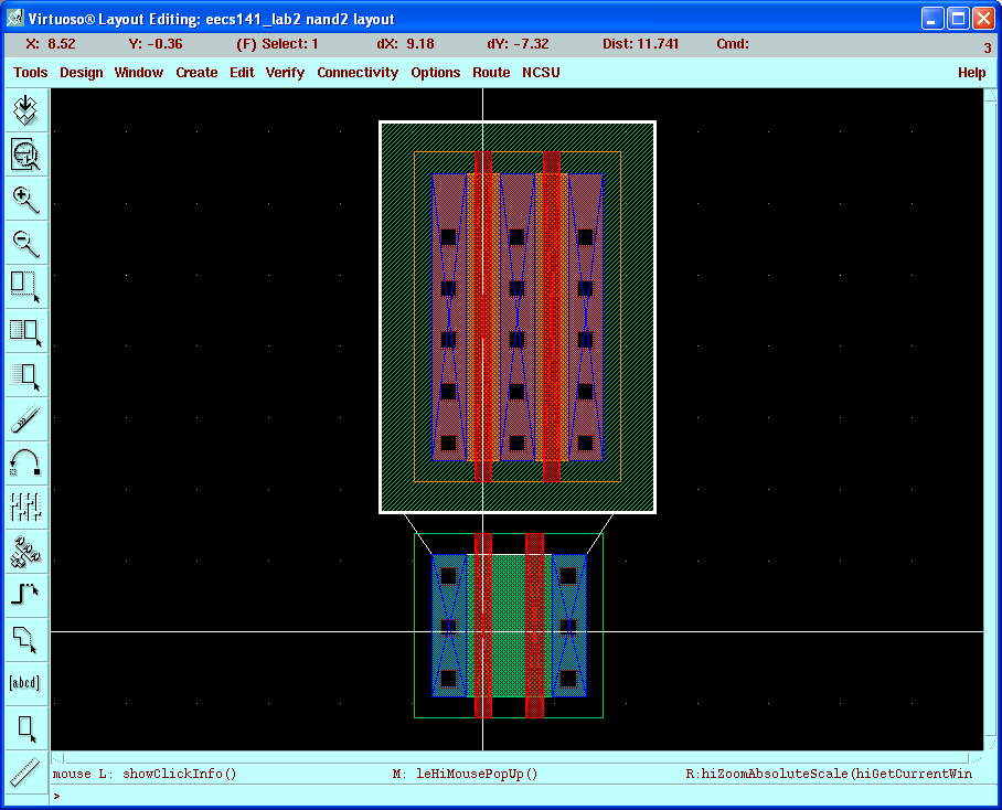
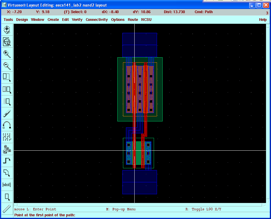
Bigger Designs and Hierarchy
Now let's use our NAND gate and an
inverter (which you need to create. Hint: simply copy and modify the NAND...)
cell to build something a little bigger.
- In the Library Manager, create new
cell named "row"
You should now be editing layout view of
"row" cell.
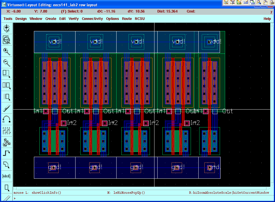
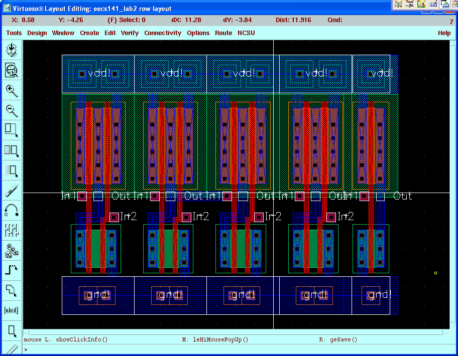
Instantiate NAND four times and inverter once to form an array of cascaded
cells.
Your layout will look something like the figure above unless you selected
to view all the internal layers.
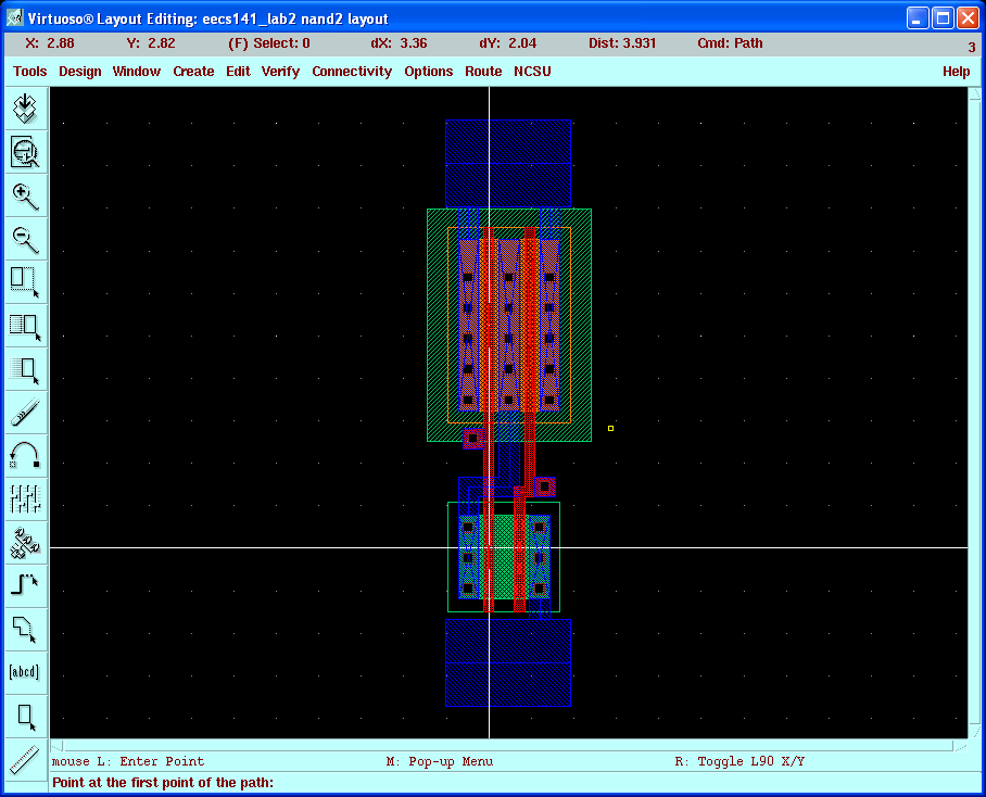
Show/Hide
Internals
You may now want to see what's inside of
the NAND2 cells and the inverter.
- To do this, hit hotkey e and
set Display Levels from 0 to 10, for example.
- This will show all the layers inside the cells as shown below:
Push, Pop, and Edit in Place
OK, now that we are here, let's say our
boss comes over and says "sorry but you need to double the number of
substrate/well contacts".
- First, select the nand cell using
and hit hotkey x (for Design - Hierarchy - Edit in Place).
- Add new taps.
- Save the cell and type B
(capital!) to get back up.
- Notice that all four instances will
be updated -- this is expected since you modified NAND cell from your
library. You can open NAND cell to check this
out).
Your layout should look something like this:
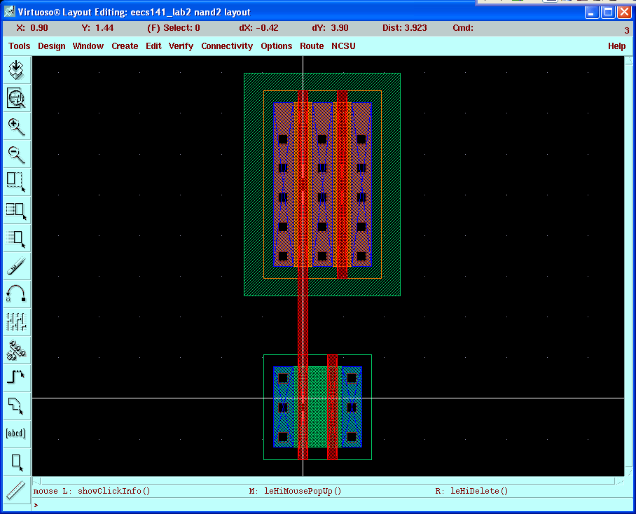
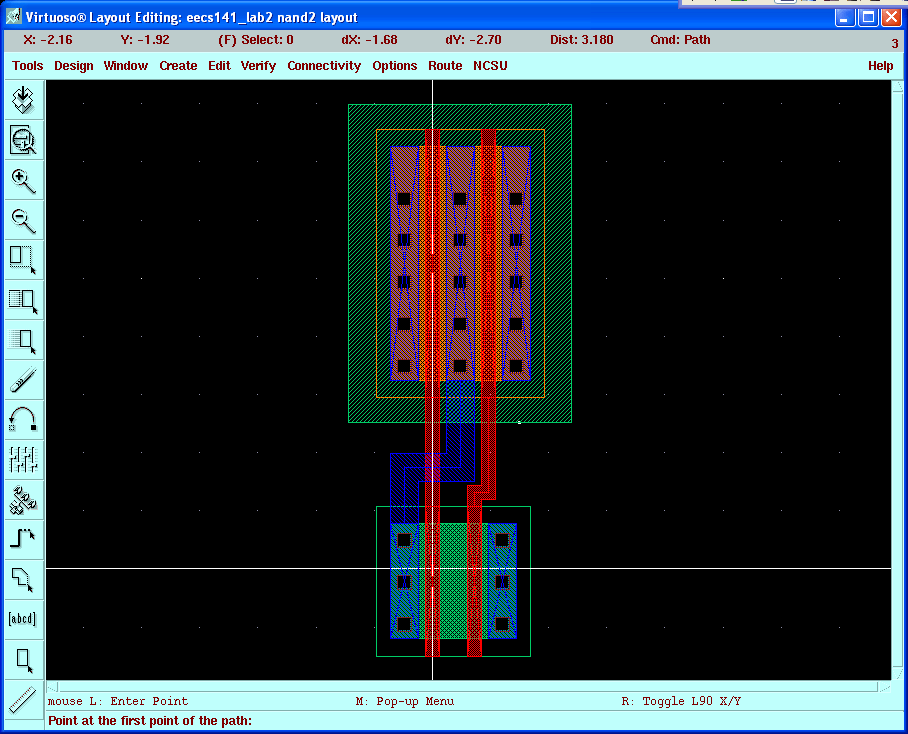
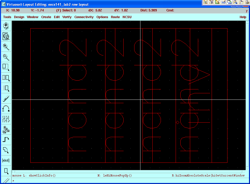
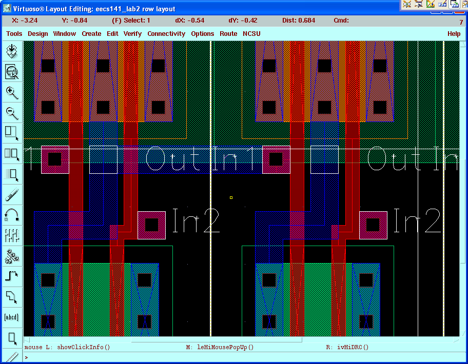
Now, just for grins, let's wire up
two of the gates. Since we want to wire them up in row and NOT in NAND
or inverter, we must first make sure row is our edit cell.
- Now that row is your edit cell,
simply use wiring strategy you learned in this tutorial to hook up a couple
of wires.
Figure below shows a zoomed in view
to show two gates wired up within row cell .
To Learn More About Virtuoso and
Analog Artist (Schematic Editor)
To learn more about Virtuoso and other
tools just type cdsdoc at your Unix prompt, and the documentation
browser should appear.
And, as always, the best way to
really learn a program is to use it!
|
