|
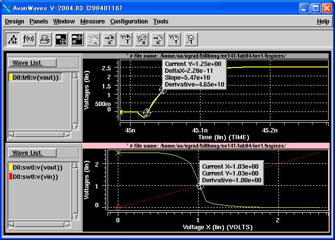
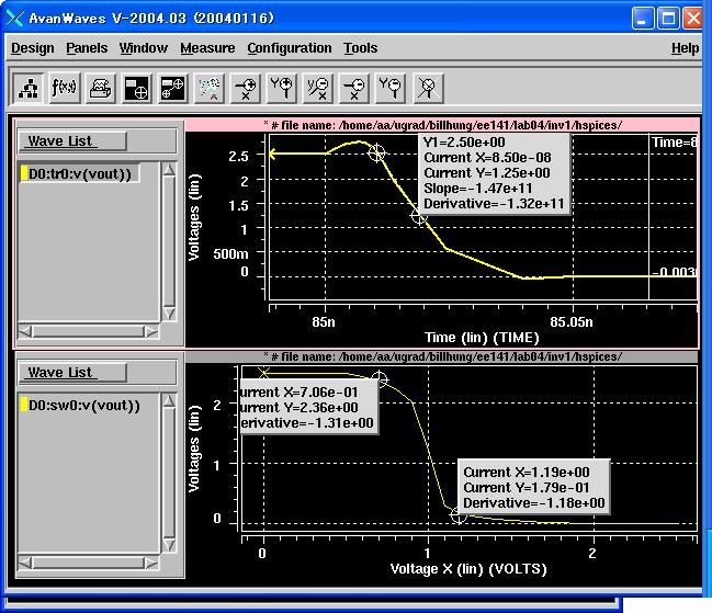
Part f L->H (PDF)
Part f H->L (PDF)
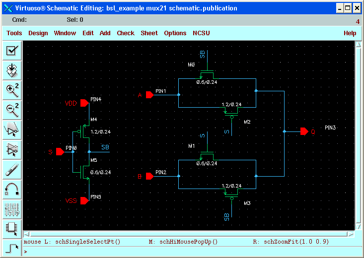
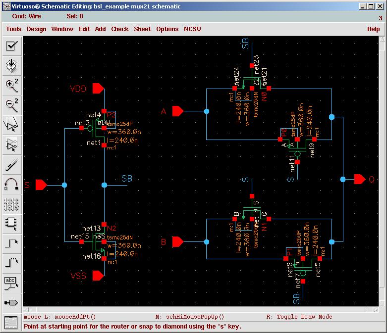
2:1 Mux Schematic
2:1 Mux Symbol
4:1 Mux Schematic
4:1 Mux Symbol
Resizing, Finding Cint
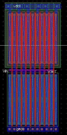
110% delay with Cload of 50fF Inverter Layout
110% delay with Cload of 50fF Inverter HSPICE
Verification
* # FILE NAME: /HOME/AA/UGRAD/BILLHUNG/EE141/LAB04/INV1/HSPICES/EXTRACTED/
* NETLIST/INV1.C.RAW
* NETLIST OUTPUT FOR HSPICES.
* GENERATED ON FEB 23 13:40:45 2006
* FILE NAME: INVERTER_INV1_EXTRACTED.S.
* SUBCIRCUIT FOR CELL: INV1.
* GENERATED FOR: HSPICES.
* GENERATED ON FEB 23 13:40:45 2006.
* INCLUDE FILES
.lib 'g25.mod' TT
* params = vlow vhigh delay rise fall pulse_width period
* example VIN IN GND PULSE 0 5 .5n .1n .1n .5n 2n
VIN VIN 0 PULSE 0 2.5 5n 10p 10p 40n 80n
VDD VDD! 0 2.5
M0 VOUT VIN VDD! VDD! PMOS L=240E-9 W=600E-9 AD=360.000007235128E-15
+AS=360.000007235128E-15 PD=1.7999999499807E-6 PS=1.7999999499807E-6 M=1
M1 VOUT VIN 0 0 NMOS L=240E-9 W=600E-9 AD=360.000007235128E-15
+AS=360.000007235128E-15 PD=1.7999999499807E-6 PS=1.7999999499807E-6 M=1
* ANALYSIS
.tran 1ns 100ns
.dc VIN 0 2.5 0.1
* END OF NETLIST
.TEMP 25.0000
.OP
.save
.option nomod post
*.OPTION INGOLD=2 ARTIST=2 PSF=2
*+ PROBE=0
.END
* # FILE NAME: /HOME/AA/UGRAD/BILLHUNG/EE141/LAB04/INV1/HSPICES/EXTRACTED/
* NETLIST/INV1.C.RAW
* NETLIST OUTPUT FOR HSPICES.
* GENERATED ON FEB 23 13:40:45 2006
* FILE NAME: INVERTER_INV1_EXTRACTED.S.
* SUBCIRCUIT FOR CELL: INV1.
* GENERATED FOR: HSPICES.
* GENERATED ON FEB 23 13:40:45 2006.
M0 VOUT VIN VDD! VDD! TSMC25DP L=240E-9 W=600E-9 AD=360.000007235128E-15
+AS=360.000007235128E-15 PD=1.7999999499807E-6 PS=1.7999999499807E-6 M=1
M1 VOUT VIN 0 0 TSMC25DN L=240E-9 W=600E-9 AD=360.000007235128E-15
+AS=360.000007235128E-15 PD=1.7999999499807E-6 PS=1.7999999499807E-6 M=1
* INCLUDE FILES
* END OF NETLIST
.TEMP 25.0000
.OP
.save
.OPTION INGOLD=2 ARTIST=2 PSF=2
+ PROBE=0
.END
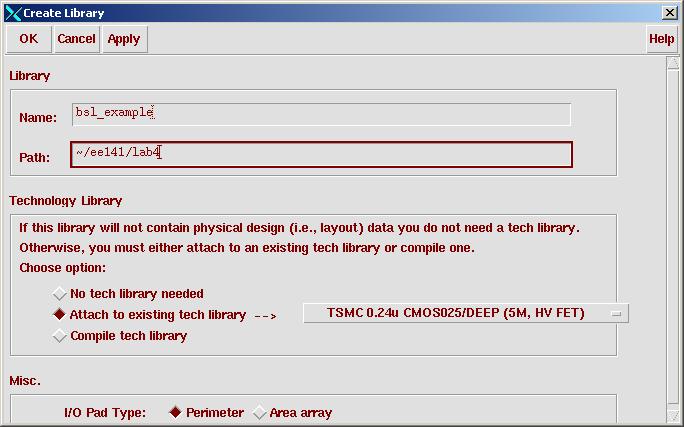
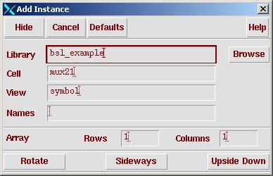
In Lab5, the name is "bsl_example". the path is "~/ee141/lab4"
new library "bsl_example"
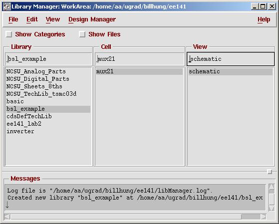
cell "mux21" view schematic
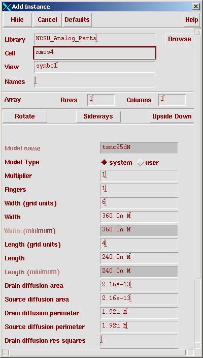
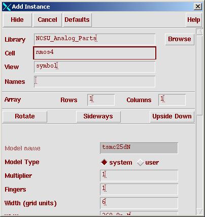
get an instance of nmos4, trying to get the schematics like below. For pmos,
type "pmos4" in Cell.
http://bwrc.eecs.berkeley.edu/classes/icdesign/ee141_s06/CadenceLabs/hierarchy/hierarchy.htm
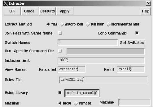
Extract
SPICE netlist from Cadence
a.
Open
the inverter layout in
Cadence and extract the layout by clicking Verify -> Extract…
on the
menu. The extraction menu should come up
and should look like the picture below. Make sure flat is
selected from Extract
Method. In the CIW there will be many commands, at the bottom there
should
“Total errors found: 0”. If you look in your Library Manager, there
should be
an additional view for your cell, extracted.
b.
Examine
the extracted
inverter view. There will be simple outlines designating different
layers in
the layout. The blue polygons are the metal 1 wires, green outlines
represent
active area, red strips are poly, and orange boxes represent contacts.
You
should also see large red boxes and bold white lines that stand out
from the
outlines. These are the ports of your devices and the nets that connect
them.
c.
To
netlist the extracted
cell view, you will need to run Affirma Analog Environment by
clicking
on Tools -> Analog Environment. Analog Environment is a
graphical
interface for running and analyzing Spectre (a language similar to
SPICE)
simulations on circuits. You may find this tool useful for running
analysis on
your project. For now, we will use Analog Environment to generate SPICE
netlists. In the Affirma Analog Circuit Design Environment
window click Setup
-> Environment…. In the window that opens select hspice
from the Include/Stimulus
File Syntax field and flat in the Netlist Type
field, then
click OK. Now go to Setup ->Simulator/Directory/Host…and
change the Project
Directory field to your lab directory then press OK. If you are
prompted to
save the state, go ahead press OK. Finally, click Simulation ->
Netlist
-> Create Final in Analog Environment. You will be able to see
the
netlist commands in the CIW and a “…successful” line then your netlist
should
open in a separate window.
d.
Now
go back to your command
line and in your lab directory go to CELLNAME/hspiceS/extracted/netlist
where
CELLNAME is the name of your cell. In that directory, your
extracted
netlist will be called hspiceFinal. Examine the netlist and you
will see
all the MOS transistors. Make sure the NMOS and PMOS have the correct
width,
length, drain and source area, and perimeters.
e.
We
will not be using the
NCSU model libraries, so comment out the lines:
.lib
"/ncsu/cadence/local/models/hspice/public/publicModel/tsmc25dP" PMOS
.lib
"/ncsu/cadence/local/models/hspice/public/publicModel/tsmc25dN"
NMOS
if they are
present. Copy the EE141 spice model for TSMC 0.25 to the
lab directory.
> cp ~ee141/MODELS/g25.mod .
Then add the line to reference the library,
.lib ‘g25.mod’
TT
for EE141 models.
Change the NMOS and PMOS models from the “TSMC25DN”
“TSMC25DP” to “NMOS” and “PMOS”, respectively. Finally comment out the
Analog
Artist options:
.OPTION
INGOLD=2 ARTIST=2 PSF=2
+
PROBE=0
Hierarchical schematic entry in
Composer
http://bwrc.eecs.berkeley.edu/classes/icdesign/ee141_s06/CadenceLabs/hierarchy/hierarchy.htm
"i", create nmos
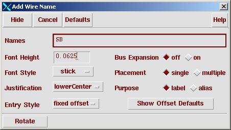
"r" rotate, "w" wire, Add->Pin or "p" to put down pins. "l" to label
wires in schematic
Done drawing the schematic. Schematic check completed with no errors.
Create Symbol View
Design-Create Cellview->Form Cellview
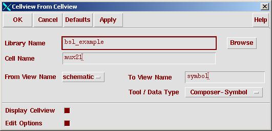
"OK"
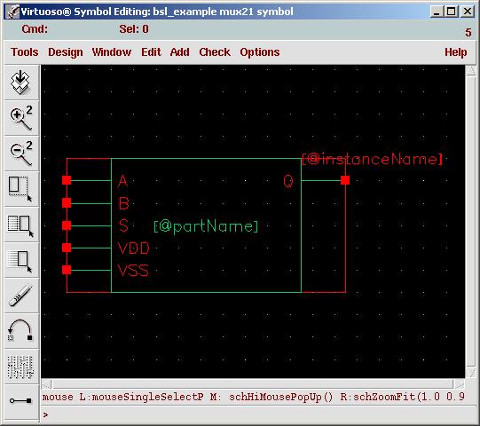
Delete green box, redraw, move wires around.
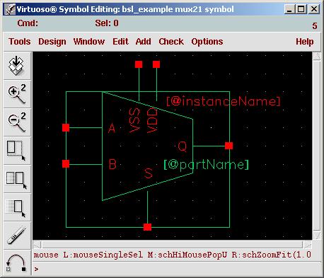
Done.
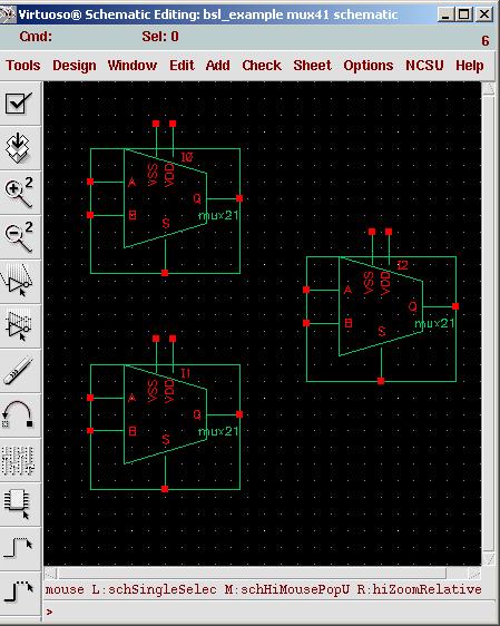
Create 4:1 mux
In library manager. Cell=mux41, View=schematic.
Instantiate three 2:1 mux cell.
Put pins, wires, and labels. "p" then D<3:0> for pin name. Output
pin Q.
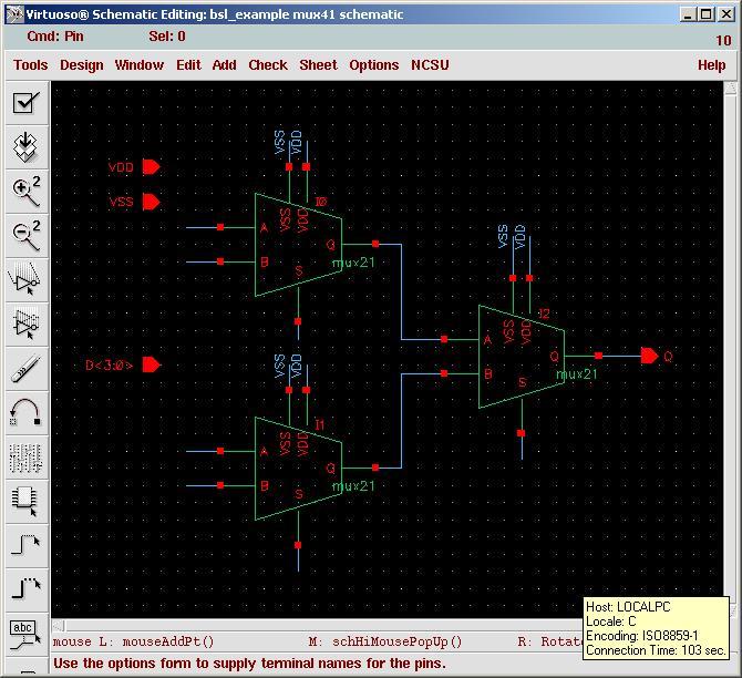
Then wire the 4 input wires separately. "l" then name the wires
<1><2><3><4>.
Create S<0:1> for control bits, and "l" for S<0> and
S<1>
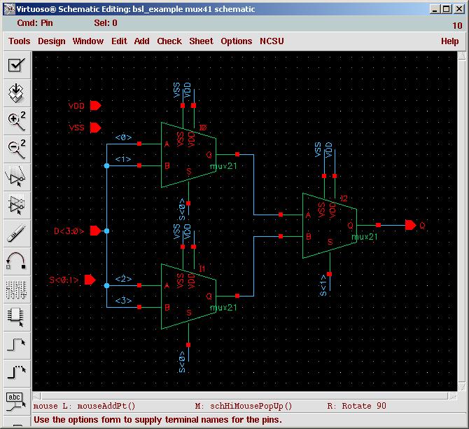
Done. Schematic check completed with no errors.
Make 4:1 mux symbole. Design-> Create Cellview->From Cellveiw.
"OK"
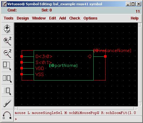
Redraw the symbol.
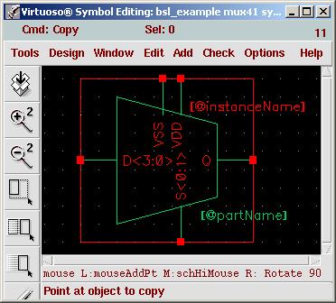
Done. Schematic check completed with no errors.
Extrace Cint from hspice netlist
Cint_inverter.sp
Extract Cint for calculation of sizing parameter
.lib 'g25.mod' TT
*****************************************
* Circuit
* vdd
* |
* in---(Inverter)---out
*
|
|
*(VIN)
C1
*
|
|
*
0
0
*****************************************
* Parameter
*****************************************
.param vddp=2.5
.param cload=100fF
*****************************************
* Netlist
*****************************************
* params = vlow vhigh delay rise fall pulse_width period
* example VIN IN GND PULSE 0 5 .5n .1n .1n .5n 2n
VIN in 0 PULSE 0 2.5 5n 10p 10p 40n 80n
VDD vdd 0 'vddp'
C1 out 0 'cload'
.subckt INV VDD! GND VIN VOUT
*M<name> <drain> <gate> <source> <bulk>
<model> <geometry>
M0 VOUT VIN VDD! VDD! PMOS L=240E-9 W=600E-9
AD=360.000007235128E-15
+AS=360.000007235128E-15 PD=1.7999999499807E-6 PS=1.7999999499807E-6
M=1
M1 VOUT VIN GND GND NMOS L=240E-9 W=600E-9
AD=360.000007235128E-15
+AS=360.000007235128E-15 PD=1.7999999499807E-6 PS=1.7999999499807E-6
M=1
.ends
Xinv1 vdd 0 in out INV
*****************************************
* Analysis
*****************************************
*nomod= no model info from library
.option nomod post=2
.meas tfall trig v(in) val='vddp/2' cross=1 targ v(in) val='vddp/2'
cross=1
.tran 0.01ns 1ns sweep cload 0f 100f 1f
*****************************************
* END OF NETLIST
******************************************
.TEMP 25.0000
*.op makes hspice determines DC operating point
.OP
.save
.END
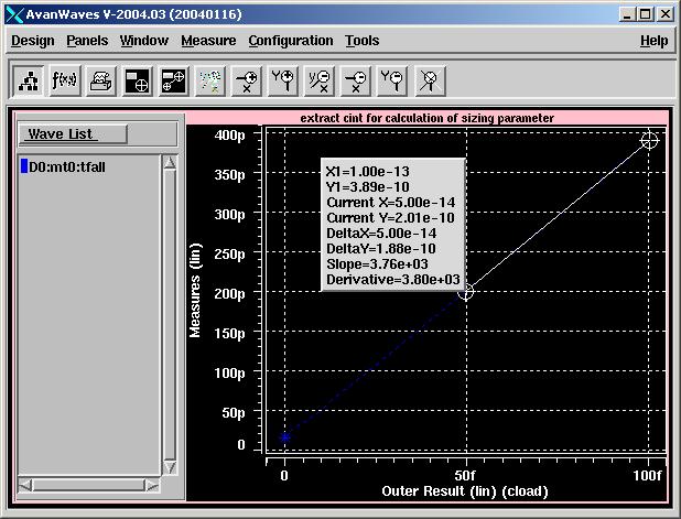
Cint = 2.01e-10 / 3.80e3 - 5e-14 = 2.895 fF

Press Verify -> Extract
Make sure flat is selected from Extract Method. Do Design Rule check (DRC).
"OK"
Total errors found: 0
The layout looks like this.
To netlist the extracted cell view, you will need to run Affirma Analog
Environment by
clicking on Tools -> Analog Environment. Analog Environment is a graphical
interface
for running and analyzing Spectre (a language similar to SPICE) simulations on
circuits.
You may find this tool useful for running analysis on your project. For now, we
will use
Analog Environment to generate SPICE netlists. In the Affirma Analog Circuit
Design
Environment window click Setup -> Environment. In the window that opens select
hspice from the Include/Stimulus File Syntax field and flat in the Netlist Type
field, then
click OK. Now go to Setup ->Simulator/Directory/Host and change the Project
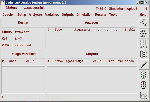
...successful.
Now go back to your command line and in your lab directory go to
CELLNAME/hspiceS/extracted/netlist where CELLNAME is the name of your cell.
In that directory, your extracted netlist will be called hspiceFinal.
We will not be using the NCSU model libraries, so comment out the lines:
.lib "/ncsu/cadence/local/models/hspice/public/publicModel/tsmc25dP" PMOS
.lib "/ncsu/cadence/local/models/hspice/public/publicModel/tsmc25dN" NMOS
if they are present. Copy the EE141 spice model for TSMC 0.25 to the lab
directory.
> cp ~ee141/MODELS/g25.mod .
Then add the line to reference the library,
.lib "g25.mod" TT
for EE141 models. Change the NMOS and PMOS models from the ?TSMC25DN?
?TSMC25DP? to ?NMOS? and ?PMOS?, respectively. Finally comment out the Analog
Artist options:
.OPTION INGOLD=2 ARTIST=2 PSF=2
+ PROBE=0
* # FILE NAME: /HOME/AA/UGRAD/BILLHUNG/CADENCE/SIMULATION/INV3/HSPICES/
* EXTRACTED/NETLIST/INV3.C.RAW
* NETLIST OUTPUT FOR HSPICES.
* GENERATED ON MAR 10 19:58:20 2006
M0 1 4 3 1 TSMC25DP L=240E-9 W=10.38E-6 AD=6.22799988664324E-12
+AS=3.73679993198595E-12 PD=11.580000318645E-6 PS=720.000002729648E-9 M=1
M1 3 4 1 1 TSMC25DP L=240E-9 W=10.38E-6 AD=3.73679993198595E-12
+AS=3.73679993198595E-12 PD=720.000002729648E-9 PS=720.000002729648E-9 M=1
M2 1 4 3 1 TSMC25DP L=240E-9 W=10.38E-6 AD=3.73679993198595E-12
+AS=3.73679993198595E-12 PD=720.000002729648E-9 PS=720.000002729648E-9 M=1
M3 3 4 1 1 TSMC25DP L=240E-9 W=10.38E-6 AD=3.73679993198595E-12
+AS=3.73679993198595E-12 PD=720.000002729648E-9 PS=720.000002729648E-9 M=1
M4 1 4 3 1 TSMC25DP L=240E-9 W=10.38E-6 AD=3.73679993198595E-12
+AS=3.73679993198595E-12 PD=720.000002729648E-9 PS=720.000002729648E-9 M=1
M5 3 4 1 1 TSMC25DP L=240E-9 W=10.38E-6 AD=3.73679993198595E-12
+AS=3.73679993198595E-12 PD=720.000002729648E-9 PS=720.000002729648E-9 M=1
M6 1 4 3 1 TSMC25DP L=240E-9 W=10.38E-6 AD=3.73679993198595E-12
+AS=3.73679993198595E-12 PD=720.000002729648E-9 PS=720.000002729648E-9 M=1
M7 3 4 1 1 TSMC25DP L=240E-9 W=10.38E-6 AD=3.73679993198595E-12
+AS=3.73679993198595E-12 PD=720.000002729648E-9 PS=720.000002729648E-9 M=1
M8 1 4 3 1 TSMC25DP L=240E-9 W=10.38E-6 AD=3.73679993198595E-12
+AS=3.73679993198595E-12 PD=720.000002729648E-9 PS=720.000002729648E-9 M=1
M9 3 4 1 1 TSMC25DP L=240E-9 W=10.38E-6 AD=3.73679993198595E-12
+AS=6.22799988664324E-12 PD=720.000002729648E-9 PS=11.580000318645E-6 M=1
M10 2 4 3 2 TSMC25DN L=240E-9 W=10.38E-6 AD=6.22799988664324E-12
+AS=3.73679993198595E-12 PD=11.580000318645E-6 PS=720.000002729648E-9 M=1
M11 3 4 2 2 TSMC25DN L=240E-9 W=10.38E-6 AD=3.73679993198595E-12
+AS=3.73679993198595E-12 PD=720.000002729648E-9 PS=720.000002729648E-9 M=1
M12 2 4 3 2 TSMC25DN L=240E-9 W=10.38E-6 AD=3.73679993198595E-12
+AS=3.73679993198595E-12 PD=720.000002729648E-9 PS=720.000002729648E-9 M=1
M13 3 4 2 2 TSMC25DN L=240E-9 W=10.38E-6 AD=3.73679993198595E-12
+AS=3.73679993198595E-12 PD=720.000002729648E-9 PS=720.000002729648E-9 M=1
M14 2 4 3 2 TSMC25DN L=240E-9 W=10.38E-6 AD=3.73679993198595E-12
+AS=3.73679993198595E-12 PD=720.000002729648E-9 PS=720.000002729648E-9 M=1
M15 3 4 2 2 TSMC25DN L=240E-9 W=10.38E-6 AD=3.73679993198595E-12
+AS=3.73679993198595E-12 PD=720.000002729648E-9 PS=720.000002729648E-9 M=1
M16 2 4 3 2 TSMC25DN L=240E-9 W=10.38E-6 AD=3.73679993198595E-12
+AS=3.73679993198595E-12 PD=720.000002729648E-9 PS=720.000002729648E-9 M=1
M17 3 4 2 2 TSMC25DN L=240E-9 W=10.38E-6 AD=3.73679993198595E-12
+AS=3.73679993198595E-12 PD=720.000002729648E-9 PS=720.000002729648E-9 M=1
M18 2 4 3 2 TSMC25DN L=240E-9 W=10.38E-6 AD=3.73679993198595E-12
+AS=3.73679993198595E-12 PD=720.000002729648E-9 PS=720.000002729648E-9 M=1
M19 3 4 2 2 TSMC25DN L=240E-9 W=10.38E-6 AD=3.73679993198595E-12
+AS=6.22799988664324E-12 PD=720.000002729648E-9 PS=11.580000318645E-6 M=1
* INCLUDE FILES
* END OF NETLIST
.TEMP 25.0000
.OP
.save
.OPTION INGOLD=2 ARTIST=2 PSF=2
+ PROBE=0
.END
* # FILE NAME: /HOME/AA/UGRAD/BILLHUNG/CADENCE/SIMULATION/INV3/HSPICES/
* EXTRACTED/NETLIST/INV3.C.RAW
* NETLIST OUTPUT FOR HSPICES.
* GENERATED ON MAR 10 19:58:20 2006
M0 1 4 3 1 PMOS L=240E-9 W=10.38E-6 AD=6.22799988664324E-12
+AS=3.73679993198595E-12 PD=11.580000318645E-6 PS=720.000002729648E-9 M=1
M1 3 4 1 1 PMOS L=240E-9 W=10.38E-6 AD=3.73679993198595E-12
+AS=3.73679993198595E-12 PD=720.000002729648E-9 PS=720.000002729648E-9 M=1
M2 1 4 3 1 PMOS L=240E-9 W=10.38E-6 AD=3.73679993198595E-12
+AS=3.73679993198595E-12 PD=720.000002729648E-9 PS=720.000002729648E-9 M=1
M3 3 4 1 1 PMOS L=240E-9 W=10.38E-6 AD=3.73679993198595E-12
+AS=3.73679993198595E-12 PD=720.000002729648E-9 PS=720.000002729648E-9 M=1
M4 1 4 3 1 PMOS L=240E-9 W=10.38E-6 AD=3.73679993198595E-12
+AS=3.73679993198595E-12 PD=720.000002729648E-9 PS=720.000002729648E-9 M=1
M5 3 4 1 1 PMOS L=240E-9 W=10.38E-6 AD=3.73679993198595E-12
+AS=3.73679993198595E-12 PD=720.000002729648E-9 PS=720.000002729648E-9 M=1
M6 1 4 3 1 PMOS L=240E-9 W=10.38E-6 AD=3.73679993198595E-12
+AS=3.73679993198595E-12 PD=720.000002729648E-9 PS=720.000002729648E-9 M=1
M7 3 4 1 1 PMOS L=240E-9 W=10.38E-6 AD=3.73679993198595E-12
+AS=3.73679993198595E-12 PD=720.000002729648E-9 PS=720.000002729648E-9 M=1
M8 1 4 3 1 PMOS L=240E-9 W=10.38E-6 AD=3.73679993198595E-12
+AS=3.73679993198595E-12 PD=720.000002729648E-9 PS=720.000002729648E-9 M=1
M9 3 4 1 1 PMOS L=240E-9 W=10.38E-6 AD=3.73679993198595E-12
+AS=6.22799988664324E-12 PD=720.000002729648E-9 PS=11.580000318645E-6 M=1
M10 2 4 3 2 NMOS L=240E-9 W=10.38E-6 AD=6.22799988664324E-12
+AS=3.73679993198595E-12 PD=11.580000318645E-6 PS=720.000002729648E-9 M=1
M11 3 4 2 2 NMOS L=240E-9 W=10.38E-6 AD=3.73679993198595E-12
+AS=3.73679993198595E-12 PD=720.000002729648E-9 PS=720.000002729648E-9 M=1
M12 2 4 3 2 NMOS L=240E-9 W=10.38E-6 AD=3.73679993198595E-12
+AS=3.73679993198595E-12 PD=720.000002729648E-9 PS=720.000002729648E-9 M=1
M13 3 4 2 2 NMOS L=240E-9 W=10.38E-6 AD=3.73679993198595E-12
+AS=3.73679993198595E-12 PD=720.000002729648E-9 PS=720.000002729648E-9 M=1
M14 2 4 3 2 NMOS L=240E-9 W=10.38E-6 AD=3.73679993198595E-12
+AS=3.73679993198595E-12 PD=720.000002729648E-9 PS=720.000002729648E-9 M=1
M15 3 4 2 2 NMOS L=240E-9 W=10.38E-6 AD=3.73679993198595E-12
+AS=3.73679993198595E-12 PD=720.000002729648E-9 PS=720.000002729648E-9 M=1
M16 2 4 3 2 NMOS L=240E-9 W=10.38E-6 AD=3.73679993198595E-12
+AS=3.73679993198595E-12 PD=720.000002729648E-9 PS=720.000002729648E-9 M=1
M17 3 4 2 2 NMOS L=240E-9 W=10.38E-6 AD=3.73679993198595E-12
+AS=3.73679993198595E-12 PD=720.000002729648E-9 PS=720.000002729648E-9 M=1
M18 2 4 3 2 NMOS L=240E-9 W=10.38E-6 AD=3.73679993198595E-12
+AS=3.73679993198595E-12 PD=720.000002729648E-9 PS=720.000002729648E-9 M=1
M19 3 4 2 2 NMOS L=240E-9 W=10.38E-6 AD=3.73679993198595E-12
+AS=6.22799988664324E-12 PD=720.000002729648E-9 PS=11.580000318645E-6 M=1
* INCLUDE FILES
.lib '/home/ff/ee141/MODELS/g25.mod' TT
* params = vlow vhigh delay rise fall pulse_width period
* example VIN IN GND PULSE 0 5 .5n .1n .1n .5n 2n
VIN 4 0 PULSE 0 2.5 5n 10p 10p 40n 80n
VDD 1 0 2.5
VGND 2 0 0
cload 3 0 50fF
* ANALYSIS
.tran 1ns 100ns
* END OF NETLIST
.TEMP 25.0000
.OP
.save
.option nomod post=2
*.OPTION INGOLD=2 ARTIST=2 PSF=2
*+ PROBE=0
.END
| 