|
Cadence Schematic Composer
Tutorial (PDF)
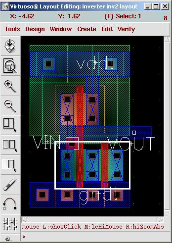
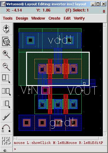
Inverter 1 Layout (PDF)
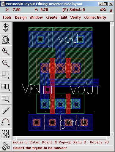
Inverter 2 Layout (PDF)
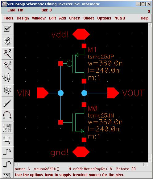
Schematic Layout (PDF)
Virtuoso Schematic Composer is a tool that allows you to create
schematics. It is useful during debugging such as cross-probing and
layout-vs-schematic checking (LVS).
Setting Up
Make a folder lab3, type icfb&
in the ee141 folder and start cadence. Tool->Library Manager.

File->New->Library in Library Manager. Note, when I type
icfb& in the ee141/lab3 folder, this step did not work. Input the
following.

"OK"
in Cell, type "inv1", in View, "layout"
Go to ~/ee141/lab3/inverter/inv1/layout/ and type "cp
~ee141/lab3/layout/* ." with the dot(.)
Overwrite the 3 files.
Close the blank layout and open the layout again.

I get a template of the lab 3.
Layout Same Sized NMOS/PMOS
Inverter (W/L)=(.6u/.24u)
Be sure to add the nwell (the pwell being implicit in this process),
and several nwell
(ntap) and pwell (ptap) contacts. The well contacts can be instantiated
from the
NCSU_TechLib_tsmc03d library. Complete the layout and eliminate any DRC
errors.
Save your results.
"i" add NCSU_TechLib_tsmc03d, nmos and pmos
change the widths to 600nm

choose poly in LSW, "r" to draw rectangle
"p" for path, path width=0.48um or 4 lambda, do DRC

"i" add NCSU_TechLib_tsmc03d, ntap and ptap. Several of them.
"p", then select metal 1 to place contact.

Complete the layout inverter using Virtuoso Layout Editor. Use
Create->Pin (Shape pin)
to label the nodes. Label the input VIN (using type “input”) and the
output VOUT (using
type “output”). Also add VDD and GND using an “inputOutput” pin type.
If you don't see anything, "e" check "Pin Name"

Done.
Plot->Submit->Plot Options
Display Type: psc
Plotter Name: local_color
Send Plot Only to File: lab03_2c.ps (Note, choose plotter name =
EPS for black and white copies)
"OK"
ps2pdf lab03_2c.ps, then
lp -d 353hp8000 lab03_2c.ps
to print the pdf file.
Layout Same Sized NMOS/PMOS
Inverter (W/L)=(1.2u/.24u)
Open another cell inv2, "c" to copy the inv1 to the empty inv2
"q" to change the width to 1.2u, you will see the pmos and nmos become
too big to fit. (The nmos has a multiplier of 2)

So change back the width to 0.6u, and put mulitiplier of 2 for nmos and
pmos. Same technique as lab 2.

"m" to move the middle stuff to the right positions.

Done.
Note that the final layout is different, see the beginning of this page.
Cadence Schematic Composer
Tutorial (PDF)

|
