|
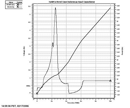
1a Fanout and Buffer Delay (PDF)
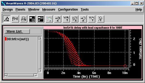
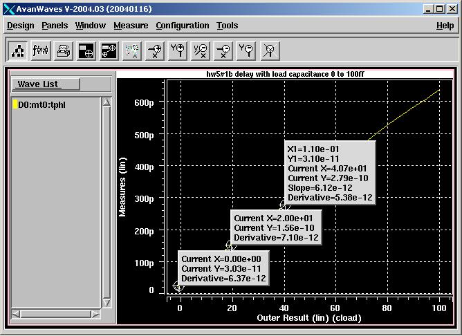
1b Delay with Load Capacitance 0 to
100fF (PDF)
1c propagation delay of one out of eight inverters (PDF)
Solution (PDF)
HW5#1a Fanout and Buffer Delay
.lib '/home/ff/ee141/MODELS/g25.mod' TT
*****************************************
* Parameter
*****************************************
.param vddp=2.5
*****************************************
* Netlist
*****************************************
VDD vdd 0 'vddp'
I 0 in 1u
.subckt INV Vdd Gnd Vin Vout
M1 Vout Vin Vdd Vdd pmos l=0.24u w=0.6u
M2 Vout Vin Gnd Gnd nmos l=0.24u w=0.36u
.ends
X1 vdd 0 in out INV
*initial conditions
.ic v(in)=0
*****************************************
* Analysis
*****************************************
.options post=2 nomod
.op
.tran 0.1ns 10ns
.end
HW5#1b Delay with Load Capacitance 0 to 100fF
.lib '/home/ff/ee141/MODELS/g25.mod' TT
*****************************************
* Circuit
* vdd
* |
* in---(Inverter)--out3
* | |
*(VIN) C1
* | |
* 0 0
*****************************************
* Parameter
*****************************************
.param vddp=2.5
.param cload=100fF
*****************************************
* Netlist
*****************************************
VDD vdd 0 'vddp'
C1 out 0 'cload*1fF'
* params = vlow vhigh delay rise fall pulse_width period
* example VIN IN GND PULSE 0 5 .5n .1n .1n .5n 2n
VIN in 0 PULSE 0 2.5 .1n .1n .1n 1u 1u
.subckt INV Vdd Gnd Vin Vout
M1 Vout Vin Vdd Vdd pmos l=0.24u w=0.6u
M2 Vout Vin Gnd Gnd nmos l=0.24u w=0.36u
.ends
X1 vdd 0 in out INV
*initial conditions
.ic v(in)=0
*****************************************
* Analysis
*****************************************
*nomod= no model info from library
.options post=2 nomod
*.op makes hspice determines DC operating point
.op
.measure tran tphl trig v(in) val='vddp/2' rise=1
+targ v(out) val='vddp/2' fall=1
.tran 0.1ns 10ns sweep cload 0 100 5
.end
HW5#1c propagation delay of one out of eight inverters
.lib '/home/ff/ee141/MODELS/g25.mod' TT
*****************************************
* Circuit
* vdd
* |
* in---(Inverter x 8)--out3
* | |
*(VIN) C1
* | |
* 0 0
*simulate a geometrically tapered chain of 8
*inverters with fanout factor f. Give a sharp
* rising edge at the input of the first inverter
*and a large capacitor loading the last. Use
*your estimate of input capacitance from part a
*to scale this load to emulate a continuation
*of the inverter chain. Measure the propagation
* delay of an inverter in the middle of the chain,
*for fanouts of 1 through 5
*****************************************
* Parameter
*****************************************
.param vddp=2.5
.param cload=10000000000000
.param f=1
*****************************************
* Netlist
*****************************************
VDD vdd 0 'vddp'
C1 out 0 'cload*1aF'
* params = vlow vhigh delay rise fall pulse_width period
* example VIN IN GND PULSE 0 5 .5n .1n .1n .5n 2n
VIN in 0 PULSE 0 2.5 .1n .1n .1n 1u 1u
.subckt INV Vdd Gnd Vin Vout
*M<name> <drain> <gate> <source> <bulk> <model> <geometry>
M1 Vout Vin Vdd Vdd pmos l=0.24u w=0.6u
M2 Vout Vin Gnd Gnd nmos l=0.24u w=0.36u
.ends
Xinv1 vdd 0 in 1 INV M='f'
Xinv2 vdd 0 1 2 INV M='f**2'
Xinv3 vdd 0 2 3 INV M='f**3'
Xinv4 vdd 0 3 4 INV M='f**4
Xinv5 vdd 0 4 5 INV M='f**5'
Xinv6 vdd 0 5 6 INV M='f**6'
Xinv7 vdd 0 6 7 INV M='f**7'
Xinv8 vdd 0 7 out INV M='f**8'
*initial conditions
.ic v(in)=0
*****************************************
* Analysis
*****************************************
*nomod= no model info from library
.options post=2 nomod
*.op makes hspice determines DC operating point
.op
.measure tran tp trig v(in) val='vddp/2' rise=1
+targ v(2) val='vddp/2' rise=1
.tran 0.1ns 10ns sweep f 1 5 1
.end
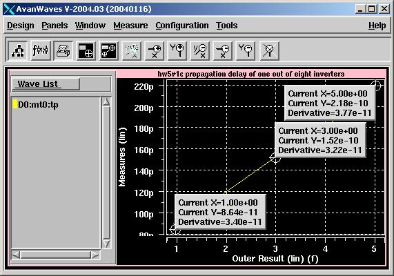
Notice the .measure is actually across 2 inverters | 