| Lab 02 Cadence Layout Tool
DOWNLOAD
Following the Cadence Layout Tool Tutorial from the beginning and built
an NMOS transistor
like the one below.

Press i, open another instance of pmos by selecting the options below

put the instance of pmos on the layout, "Shift-z" to zoom out, "m" to
move the pmos, "f" to fit the image to the screen.
"q" to edit properties. Change width to 4u (auto changed to
4.02u) and multiplier from 1 to 2.

Press "OK" on top.

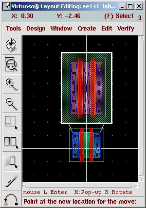
"m" to move the pmos, "f" to fit image.
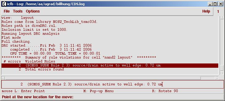
Now do a Design Rule Check
Go to the pull down menu, Verify->DRC, press OK. The layout will
indicate a DRC error, notice the little white lines between NMOS and
PMOS.
error windows explains the error.
"r", draw a retangle like the screen shot below, and "q" to change it
to poly.

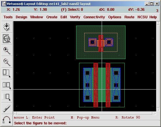
Now draw a data path. "p" to draw a fat pwell structure, then select
the pwell structure and "q" to select metal1(dg), not metal1(nt). Then
"s" to resize the width of the path to 0.48.
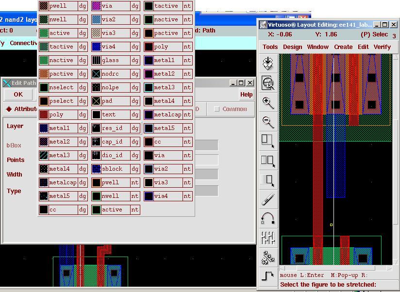
You can select the material you are drawing my clicking the materal
(like metal1 in LSW) window.
or
keep drawing poly by "r", draw a pwell, then "q" to change the pwell to
poly, multiple poly can stack together to work. "p" to draw a fat
pwell, then "q" to change to "metal1(dg)". I drew the metal shape by
dragging one signal path, instead of stacking paths like the poly. The
3 wiring (1 path, 2 poly) should look like the picture below.

Continues the Cadence Layout Tool Tutorial under the Titlle Adding the Power Rails.
Tips
1. In the Finishing Cell section, you need to have a
layer of n-well by pressing "r" in the area of the vdd! or a DRC error
will bug you.
Tools
1. "k" to use ruler, then click 2 times to take
measurements. "Shift-k"
2. "e" -> Pin Names to display pin names. Especially open an old
design, the default does not show pin names.
3. lp -d 353hp8000 lab02_plot_color.ps - This
is to print the ps file to the HP printer in Cory 353.
4. ps2pdf filename.ps - This converts your ps file to
pdf file
5. lpstat -t | grep 353 - to search printer in room
353 |
