Peter Lau
Bill Chun Wai Hung
Lab 9 Report
¨C Voltage Rectifier
A. Describe the Set-up
There
are 3 circuits in this lab, and each circuit has part I and Part II.
The Circuit 1 setup is shown in figure 1.
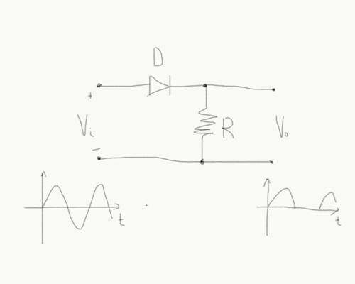
Figure 1
The
Circuit 2 setup is shown in figure 2.
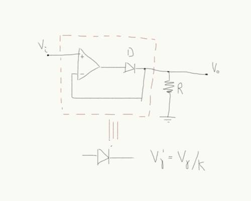
Figure 2
The
Circuit 3 setup is shown in figure 3.
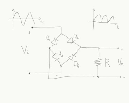
Figure 3
B. Describe Inputs
Resistor:
The Resistor used is 1k ohm
Diode:
The model for the diodes are D1N4002
Op Amp: model LM4862N
Stimuli:
For Part
I,
The +5V
and -5V voltage input is connected across the input of the circuit (Vi). The output voltage (Vo) is
measured by the DVM.
For Part
II,
The AC
function generator produce a sine curve input voltage across
the input of the circuit (Vi). The output voltage (Vo)
is measured by the oscilloscope.
C. Describe What you Observe
Part I.
Circuit
1 Simple Rectificer
The
result of V(in) (=Vi in the prelab)
versus V(out) (=Vo in the prelab) is shown in Table 1
and Figure 4 and Figure 5.
Table 1.
|
V(in)
(Volt) |
V(out)
(Volt) |
|
0.01 |
0.000 |
|
0.05 |
0.000 |
|
0.10 |
0.000 |
|
0.50 |
0.044 |
|
0.70 |
0.188 |
|
1.00 |
0.450 |
|
1.20 |
0.636 |
|
1.40 |
0.823 |
|
1.60 |
1.014 |
|
2.00 |
1.399 |
Part I
Circuit 2 Precision Rectificer.
The
result of V(in) (=Vi in the prelab)
versus V(out) (=Vo in the prelab) is shown in Table 2
and Figure 4 and Figure 5.
Table 2.
|
V(in)
(Volt) |
V(out)
(Volt) |
|
0.01 |
0.012 |
|
0.05 |
0.052 |
|
0.10 |
0.102 |
|
0.50 |
0.531 |
|
0.70 |
0.722 |
|
1.00 |
1.031 |
|
1.20 |
1.222 |
|
1.40 |
1.422 |
|
1.60 |
1.625 |
|
2.00 |
2.031 |
Part I Circuit
3 Bridge Rectificer.
The
result of V(in) (=Vi in the prelab)
versus V(out) (=Vo in the prelab) is shown in Table 3
and Figure 4 and Figure 5.
Table 3.
|
V(in)
(Volt) |
V(out)
(Volt) |
|
0.01 |
0.003 |
|
0.05 |
0.003 |
|
0.10 |
0.003 |
|
0.50 |
0.003 |
|
0.70 |
0.006 |
|
1.00 |
0.075 |
|
1.20 |
0.218 |
|
1.40 |
0.360 |
|
1.60 |
0.523 |
|
2.00 |
0.875 |

Figure 4
Part II.
Circuit 1
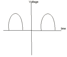
Figure 5. Circuit I and Circuit II Oscilloscope output
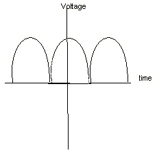
Figure 6. Circuit III Oscilloscope output
Circuit
I. V(peak to peak) = 2V, the V(out peak voltage) =
0.435V
Circuit
II. V(peak to peak) = 2V, the V(out peak voltage) =
1.062V
Circuit
III. V(peak to peak) = 6V, the V(out peak voltage) =
1.766V
D. What you can deduce
Q1) What is the difference between the half wave rectifier and the precision rectifier?
The half wave rectifier truncates one half of the sine wave plus an extra 0.6V, owing to the fixed voltage drop across the diode. The full wave rectifier circuit does not exhibit this behavior.
Q2) Why is the threshold of the precision rectifier lower than the threshold of the simple rectifier?
The output is connected to the inverting input, while the input is fed into the non-inverting input. The two inputs of an opamp are held at the same voltage by the feedback loop. This is why the output tracks the input precisely (without a voltage drop) when the diode is forward biased. Current cannot flow at all when the diode is reverse biased, so the feedback loop is broken and the input is blocked and not reflected in the output.
Q3) What is the minimum signal needed at the input of the diodes bridge in order to be able to see an output
The experimental minimum signal needed at the input of the diodes is 1 voltage. The minimum voltage input is shown in Figure 5 with the lowest curve on the plot.
Q4) Justify your answer to question Q3.
The experimental minimum input voltage agrees with the expected is minimum
input voltage = 0.5 x 2 = 1V. The
0.5V is the cutoff voltage of each diodes, and there
are two active diodes acting on the current in the circuit, so the minimum
input voltage is 1V.
What I
am planning to do in order to claim my circuit works.
Part
I Circuit 1. The middle curve in figure 4 with minimum input voltage of 0.5V
indicates one active diode in the circuit.
Part
I Circuit 2. The top curve in figure 4 with minimum input voltage of almost 0V
indicates the op amp and diode pair acting as a perfect diode.
Part
I Circuit 3. The bottom curve in figure 4 with minimum input voltage of 1V
indicates two active diode in the circuit.
Part II Circuit 1.
The output waveform is like the one in Figure 5
Part II Circuit 2.
The output waveform is like the one in Figure 5
Part II Circuit 3.
The output waveform is like the one in Figure 6