Peter Lau
Bill Chun Wai Hung
Lab 8 Report
¨C Tone Controller (Amplified)
A. Describe the Set-up
The
setup is shown in figure 1.
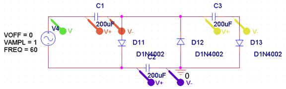
Figure 1
B. Desbribe Inputs
Stimuli:
Vin Amplitude= 1V
V
frequency is set to be 60Hz
C1 = C2
= C3 = 200uF
The model for the diodes are D1N4002
C. Describe What you Observe
The
circuit generated an experimental voltage values shown in Figure 2.

Figure 2
The Output
of the stimulation is consistent with the expected result.
The 1.0V
to -1.0V sine curve is the voltage across the input voltage.The
stepping up curve is voltage across Vc3. The other two curves are voltage
across Vc1 and Vc2 accordingly. The Vc1 is the curve that has the lower average
voltage as time increase, while the Vc2 is the curve that has the high average
voltage as time increase.
The
result shown in this graph is very similar to that of the prelab.
D. What you can deduce
What I
am planning to do in order to claim my circuit works:
The circuit works because the result of the pspice
stimulation agrees with the result of the prelab. The
input voltage is a sine curve, and the capacitance of C1 and C2 charge up and
discharge. The C3 charges up set by step.
Q1) You have tried two different
capacitance values. Are the results different? Explain why.
Yes, the results are different in the real case, but the results
should be the same in the ideal case. In the ideal case, when the diodes conducts, the diodes do not have any resistance, and
the resistance of the diode when the diode conducts are 0 ohm. However, in the
real case, the diodes used have a small resistance.
Therefore, because q=CV, so when the capacitance is increased (in
this example, from 200uF to 100mF), the voltage change of the capacitors are a
lot smaller. This is because the charge increases with the capacitance, so the
current is a lot larger. Since the diodes are not ideal and the diodes have a
small resistances. The voltage drop (non-ideal loss of voltage) across the
diodes will make the voltage change of the capacitors a lot smaller.
The result of using 100mF capacitances for C1, C2, and C3 is shown
in Figure 3. This stimulation of Figure 3 agrees with our prediction of a lower
peak to peak voltage of capacitances compared to Figure 2.

Figure 3.
And Gate Circuit.
The circuit that is built during the lab agrees with the predicted
values.
Table 1
|
Input 1 |
Input 2 |
AND gate Output |
LED
Output |
|
0 |
0 |
0 |
0 |
|
0 |
1 |
0 |
0 |
|
1 |
0 |
0 |
0 |
|
1 |
1 |
1 |
1 |
In this lab, negative logic is used. When the input is 0V, that is the same of signal 1. When the input is 5V, that is the same of signal 0.
When the LED lights up, that is the same as signal 0. When the LED
does not lights up, that is the same as signal 1.
The experimental result of the AND gate agrees with the predicted
values in Table 1.